

ADCLK914BCPZ-R7
Overview
- Category: Integrated Circuit (IC)
- Use: Clock Generator and Distribution
- Characteristics: High-speed, Low-power, Precision
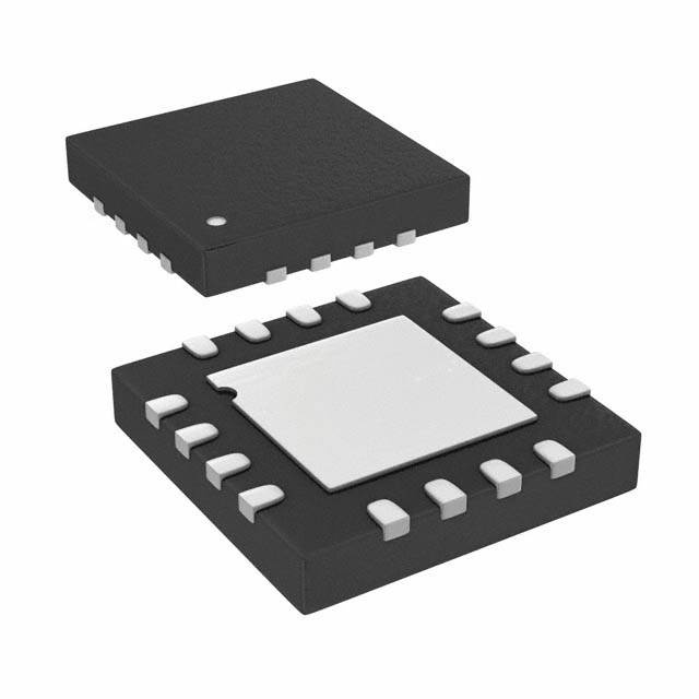
- Package: LFCSP (Lead Frame Chip Scale Package)
- Essence: High-performance clock generator and distributor
- Packaging/Quantity: Tape and Reel, 2500 units per reel
Specifications and Parameters
- Supply Voltage: 2.7V to 3.6V
- Operating Temperature Range: -40°C to +85°C
- Output Frequency Range: DC to 2.5GHz
- Output Amplitude: 800mVpp
- Power Consumption: 150mW
- Phase Noise: -155dBc/Hz at 1MHz offset
Pin Configuration
The ADCLK914BCPZ-R7 has a total of 20 pins. The pin configuration is as follows:
| Pin Number | Pin Name | Description | |------------|----------|-------------| | 1 | VDD | Power Supply Voltage | | 2 | GND | Ground | | 3 | OUT0 | Output 0 | | 4 | OUT1 | Output 1 | | 5 | OUT2 | Output 2 | | 6 | OUT3 | Output 3 | | 7 | OUT4 | Output 4 | | 8 | OUT5 | Output 5 | | 9 | OUT6 | Output 6 | | 10 | OUT7 | Output 7 | | 11 | OUT8 | Output 8 | | 12 | OUT9 | Output 9 | | 13 | OUT10 | Output 10 | | 14 | OUT11 | Output 11 | | 15 | OUT12 | Output 12 | | 16 | OUT13 | Output 13 | | 17 | OUT14 | Output 14 | | 18 | OUT15 | Output 15 | | 19 | VREF | Reference Voltage Input | | 20 | CLKIN | Clock Input |
Functional Characteristics
- High-speed clock generation and distribution
- Low-power consumption
- Precision output with low phase noise
- Wide operating temperature range
Advantages
- High-frequency capability up to 2.5GHz
- Low power consumption for energy-efficient applications
- Precise and stable clock signal generation
- Compact package size for space-constrained designs
Disadvantages
- Limited output amplitude of 800mVpp
- Requires external reference voltage for operation
Applicable Range of Products
The ADCLK914BCPZ-R7 is suitable for various applications that require high-speed clock generation and distribution, such as: - Communication systems - Data acquisition systems - Test and measurement equipment - Radar systems - Industrial automation
Working Principles
The ADCLK914BCPZ-R7 utilizes advanced circuitry to generate and distribute high-frequency clock signals. It operates by taking an input clock signal (CLKIN) and dividing it into multiple synchronized output signals (OUT0 to OUT15). The device ensures precise timing and low phase noise, making it ideal for demanding applications.
Detailed Application Field Plans
- Communication Systems: The ADCLK914BCPZ-R7 can be used in wireless communication systems to provide accurate clock synchronization between different components, ensuring reliable data transmission.
- Data Acquisition Systems: In data acquisition systems, the ADCLK914BCPZ-R7 enables precise timing for analog-to-digital converters (ADCs), ensuring accurate sampling and conversion of analog signals.
- Test and Measurement Equipment: The device is suitable for high-speed test and measurement equipment, providing synchronized clock signals for precise timing measurements.
- Radar Systems: Radar systems require accurate timing for signal processing and target detection. The ADCLK914BCPZ-R7 can generate stable clock signals to ensure reliable radar operation.
- Industrial Automation: In industrial automation applications, the device can be used to synchronize various control systems, enabling precise timing for efficient and reliable operation.
Detailed Alternative Models
- ADCLK914BCPZ-R2
- ADCLK914BCPZ-R5
- ADCLK914BCPZ-R9
- ADCLK914BCPZ-R12
- ADCLK914BCPZ-R15
5 Common Technical Questions and Answers
Q: What is the maximum output frequency of the ADCLK914BCPZ-R7? A: The ADCLK914BCPZ-R7 can generate clock signals up to 2.5GHz.
Q: Does the ADCLK914BCPZ-R7 require an external reference voltage? A: Yes