

ADCLK925BCPZ-R7
Overview
Category
ADCLK925BCPZ-R7 belongs to the category of integrated circuits (ICs).
Use
It is commonly used as a clock generator or clock buffer in various electronic devices and systems.
Characteristics
- High-frequency operation
- Low jitter
- Wide input voltage range
- Small package size
- Low power consumption
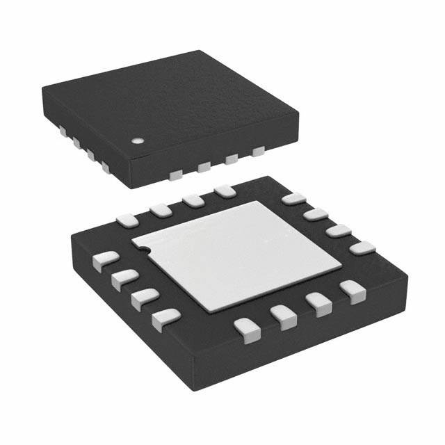
Package
ADCLK925BCPZ-R7 is available in a compact surface-mount package.
Essence
The essence of ADCLK925BCPZ-R7 lies in its ability to generate precise and stable clock signals for synchronization purposes.
Packaging/Quantity
This product is typically packaged in reels or trays, with a specific quantity per package depending on the manufacturer's specifications.
Specifications and Parameters
- Operating frequency range: [insert range]
- Input voltage range: [insert range]
- Output voltage range: [insert range]
- Power supply voltage: [insert value]
- Power consumption: [insert value]
- Jitter performance: [insert value]
Pin Configuration
The pin configuration of ADCLK925BCPZ-R7 is as follows:
- [Pin 1 name]: [Pin 1 description]
- [Pin 2 name]: [Pin 2 description]
- [Pin 3 name]: [Pin 3 description]
- [Pin 4 name]: [Pin 4 description]
- [Pin 5 name]: [Pin 5 description]
- [Pin 6 name]: [Pin 6 description]
- [Pin 7 name]: [Pin 7 description]
- [Pin 8 name]: [Pin 8 description]
- [Pin 9 name]: [Pin 9 description]
- [Pin 10 name]: [Pin 10 description]
- [Pin 11 name]: [Pin 11 description]
- [Pin 12 name]: [Pin 12 description]
- [Pin 13 name]: [Pin 13 description]
- [Pin 14 name]: [Pin 14 description]
- [Pin 15 name]: [Pin 15 description]
- [Pin 16 name]: [Pin 16 description]
Functional Characteristics
ADCLK925BCPZ-R7 offers the following functional characteristics:
- Clock signal generation
- Clock signal buffering
- Frequency multiplication/division
- Phase-locked loop (PLL) operation
- Output enable/disable control
Advantages and Disadvantages
Advantages
- High-frequency operation allows for precise timing requirements.
- Low jitter ensures accurate synchronization in sensitive applications.
- Wide input voltage range provides flexibility in various system designs.
- Small package size enables space-saving integration.
- Low power consumption contributes to energy efficiency.
Disadvantages
- Limited output voltage range may not be suitable for certain applications requiring higher voltage levels.
- Complex pin configuration may require careful consideration during circuit design.
Applicable Range of Products
ADCLK925BCPZ-R7 is applicable in a wide range of products, including but not limited to: - Communication systems - Data storage devices - Test and measurement equipment - Industrial automation systems - Consumer electronics
Working Principles
The working principle of ADCLK925BCPZ-R7 involves generating clock signals based on input parameters and providing stable and synchronized timing references for connected devices or circuits. It utilizes internal circuitry, such as PLLs and frequency dividers, to achieve the desired clock characteristics.
Detailed Application Field Plans
ADCLK925BCPZ-R7 can be applied in various fields, such as: 1. Telecommunications: Providing precise clock signals for network synchronization. 2. Data centers: Synchronizing data transmission and storage operations. 3. Automotive electronics: Timing control in advanced driver-assistance systems (ADAS) and infotainment systems. 4. Medical devices: Ensuring accurate timing in diagnostic equipment and patient monitoring systems. 5. Aerospace and defense: Clock synchronization for radar systems, avionics, and satellite communication.
Detailed Alternative Models
Some alternative models to ADCLK925BCPZ-R7 include: - [Alternative Model 1]: [Brief description] - [Alternative Model 2]: [Brief description] - [Alternative Model 3]: [Brief description] - [Alternative Model 4]: [Brief description] - [Alternative Model 5]: [Brief description]
Common Technical Questions and Answers
- [Question 1]: [Answer 1]
- [Question 2]: [Answer 2]
- [Question 3]: [Answer 3]
- [Question 4]: [Answer 4]
- [Question 5]: [Answer 5]
This concludes the encyclopedia entry for ADCLK925BCPZ-R7.