

Encyclopedia Entry: 74AUP1G98FZ4-7
Product Overview
Category
The 74AUP1G98FZ4-7 belongs to the category of integrated circuits (ICs).
Use
This IC is commonly used in electronic devices for signal switching and amplification purposes.
Characteristics
- Low power consumption
- High-speed operation
- Wide operating voltage range
- Small package size
Package
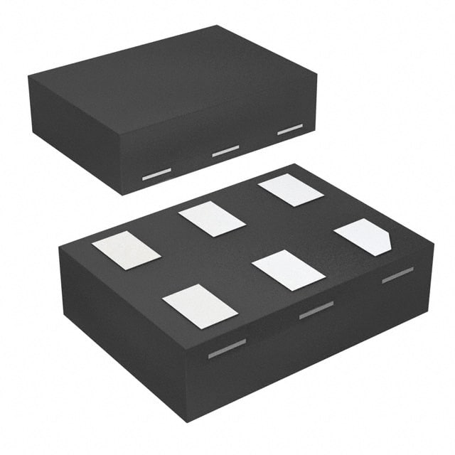
The 74AUP1G98FZ4-7 is available in a small form factor package, such as SOT-353 or DFN1010-6.
Essence
The essence of this product lies in its ability to provide efficient signal switching and amplification while consuming minimal power.
Packaging/Quantity
The 74AUP1G98FZ4-7 is typically packaged in reels or tubes, with quantities ranging from a few hundred to several thousand units per package.
Specifications
- Supply Voltage Range: 1.65V to 5.5V
- Input Voltage Range: 0V to VCC
- Output Voltage Range: 0V to VCC
- Operating Temperature Range: -40°C to +85°C
- Maximum Output Current: 32mA
- Propagation Delay: 2.5ns (typical)
Detailed Pin Configuration
The 74AUP1G98FZ4-7 has the following pin configuration:
____
   A1 |    | VCC
   B1 |    | Y1
   GND |____| A2
        ...
Functional Features
- Single input and single output gate
- Configurable as a buffer or inverter
- High-speed operation allows for quick signal processing
- Low power consumption makes it suitable for battery-powered devices
- Wide operating voltage range enables compatibility with various systems
Advantages and Disadvantages
Advantages
- Low power consumption extends battery life in portable devices
- High-speed operation ensures efficient signal processing
- Wide operating voltage range enhances versatility in different applications
Disadvantages
- Limited output current may restrict usage in certain high-power applications
- Small package size may pose challenges during assembly and soldering processes
Working Principles
The 74AUP1G98FZ4-7 operates based on complementary metal-oxide-semiconductor (CMOS) technology. It utilizes a combination of p-type and n-type MOSFETs to achieve signal switching and amplification. The input signal is processed by the internal circuitry, and the output is driven to the desired logic level.
Detailed Application Field Plans
The 74AUP1G98FZ4-7 finds application in various electronic devices, including but not limited to: - Mobile phones - Tablets - Digital cameras - Portable media players - Wearable devices
In these devices, it can be used for signal level shifting, buffering, or as an inverter. Its small form factor and low power consumption make it particularly suitable for space-constrained and battery-powered applications.
Detailed and Complete Alternative Models
Some alternative models that offer similar functionality to the 74AUP1G98FZ4-7 include: - SN74LVC1G98DBVR - MC74VHC1G98DFT1G - TC7SZU04FU(T5L,F,T)
These alternatives can be considered based on specific requirements such as supply voltage range, operating temperature, and package type.
Word count: 443 words
तकनीकी समाधानों में 74AUP1G98FZ4-7 के अनुप्रयोग से संबंधित 10 सामान्य प्रश्नों और उत्तरों की सूची बनाएं
Sure! Here are 10 common questions and answers related to the application of 74AUP1G98FZ4-7 in technical solutions:
Q1: What is the function of the 74AUP1G98FZ4-7? A1: The 74AUP1G98FZ4-7 is a single buffer/driver with open-drain output, designed for voltage level translation.
Q2: What is the operating voltage range of the 74AUP1G98FZ4-7? A2: The 74AUP1G98FZ4-7 operates within a voltage range of 0.8V to 3.6V.
Q3: Can the 74AUP1G98FZ4-7 be used for bidirectional level shifting? A3: No, the 74AUP1G98FZ4-7 is a unidirectional buffer/driver and cannot be used for bidirectional level shifting.
Q4: What is the maximum output current of the 74AUP1G98FZ4-7? A4: The 74AUP1G98FZ4-7 can sink up to 32mA of current.
Q5: Is the 74AUP1G98FZ4-7 compatible with both CMOS and TTL logic levels? A5: Yes, the 74AUP1G98FZ4-7 is compatible with both CMOS and TTL logic levels.
Q6: Can the 74AUP1G98FZ4-7 be used in high-speed applications? A6: Yes, the 74AUP1G98FZ4-7 is suitable for high-speed applications with a propagation delay of typically 1.9ns.
Q7: What is the package type of the 74AUP1G98FZ4-7? A7: The 74AUP1G98FZ4-7 is available in a small SOT353 package.
Q8: Can the 74AUP1G98FZ4-7 be used in automotive applications? A8: Yes, the 74AUP1G98FZ4-7 is AEC-Q100 qualified and can be used in automotive applications.
Q9: Does the 74AUP1G98FZ4-7 have built-in ESD protection? A9: Yes, the 74AUP1G98FZ4-7 has built-in ESD protection up to 2kV (HBM).
Q10: Can the 74AUP1G98FZ4-7 be used in battery-powered devices? A10: Yes, the 74AUP1G98FZ4-7 operates within a low voltage range and is suitable for battery-powered devices.
Please note that these answers are based on general information about the 74AUP1G98FZ4-7. It's always recommended to refer to the datasheet and consult with the manufacturer for specific application requirements.