
GD25LQ40CEIGR
Product Overview
- Category: Integrated Circuit (IC)
- Use: Non-volatile Memory
- Characteristics:
- High-speed data transfer
- Low power consumption
- Small form factor
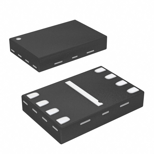
- Package: SOP8 (Small Outline Package 8)
- Essence: Flash memory chip
- Packaging/Quantity: Tape and Reel, 2500 pieces per reel
Specifications
- Memory Capacity: 4 Megabits (512 Kilobytes)
- Interface: Serial Peripheral Interface (SPI)
- Operating Voltage: 2.7V to 3.6V
- Operating Temperature: -40°C to +85°C
- Data Retention: More than 20 years
- Program/Erase Cycles: Up to 100,000 cycles
Pin Configuration
The GD25LQ40CEIGR has a total of 8 pins arranged as follows:
┌───┬───┐
   │ 1 │ 2 │
   ├───┼───┤
   │ 3 │ 4 │
   ├───┼───┤
   │ 5 │ 6 │
   ├───┼───┤
   │ 7 │ 8 │
   └───┴───┘
- Chip Select (/CS)
- Serial Clock (SCLK)
- Serial Data Input (SI)
- Serial Data Output (SO)
- Write Protect (/WP)
- Hold (/HOLD)
- Ground (GND)
- Power Supply (VCC)
Functional Features
- High-speed data transfer up to 104 MHz
- Supports both SPI mode 0 and mode 3
- Sector erase and byte/page program operations
- Software and hardware write protection options
- Deep power-down mode for low power consumption
- Auto address increment during continuous read
Advantages
- Compact size allows for easy integration into various electronic devices
- Low power consumption extends battery life in portable applications
- High-speed data transfer enables quick access to stored information
- Reliable data retention ensures long-term storage of critical data
- Flexible write protection options enhance data security
Disadvantages
- Limited memory capacity compared to larger flash memory chips
- Relatively lower program/erase cycle endurance
- Requires an external microcontroller or host device for operation
Working Principles
The GD25LQ40CEIGR is based on the Serial Peripheral Interface (SPI) protocol. It utilizes a combination of floating gate and tunnel oxide technology to store data in non-volatile memory cells. The chip communicates with a microcontroller or host device through the SPI interface, allowing for high-speed data transfer and flexible control over read, write, and erase operations.
Detailed Application Field Plans
The GD25LQ40CEIGR is widely used in various electronic devices and systems that require non-volatile memory for data storage. Some common application fields include:
Consumer Electronics:
- Smartphones
- Tablets
- Digital cameras
- Portable media players
Automotive:
- Infotainment systems
- Instrument clusters
- Advanced driver-assistance systems (ADAS)
Industrial:
- Internet of Things (IoT) devices
- Industrial automation systems
- Data loggers
- Measurement instruments
Communication:
- Routers
- Modems
- Set-top boxes
Detailed and Complete Alternative Models
Some alternative models to the GD25LQ40CEIGR with similar specifications and functionality include:
- Winbond W25Q40CL
- Macronix MX25L4006E
- Microchip SST25VF040B
- Spansion S25FL040K
These alternative models can be considered based on specific project requirements, availability, and cost considerations.
Word count: 511 words
तकनीकी समाधानों में GD25LQ40CEIGR के अनुप्रयोग से संबंधित 10 सामान्य प्रश्नों और उत्तरों की सूची बनाएं
Sure! Here are 10 common questions and answers related to the application of GD25LQ40CEIGR in technical solutions:
Question: What is GD25LQ40CEIGR?
Answer: GD25LQ40CEIGR is a serial flash memory chip manufactured by GigaDevice. It has a capacity of 4 megabits (512 kilobytes) and operates on a 3V power supply.Question: What is the interface used to communicate with GD25LQ40CEIGR?
Answer: GD25LQ40CEIGR uses the Serial Peripheral Interface (SPI) for communication with microcontrollers or other devices.Question: What are the typical applications of GD25LQ40CEIGR?
Answer: GD25LQ40CEIGR is commonly used in various electronic devices such as set-top boxes, routers, printers, and industrial control systems for storing firmware, configuration data, and other non-volatile information.Question: What is the maximum operating frequency of GD25LQ40CEIGR?
Answer: GD25LQ40CEIGR supports a maximum operating frequency of 104 MHz, allowing for fast data transfer rates.Question: Can GD25LQ40CEIGR be easily soldered onto a PCB?
Answer: Yes, GD25LQ40CEIGR comes in an industry-standard 8-pin SOIC package, which can be easily soldered onto a PCB using standard surface mount technology.Question: Does GD25LQ40CEIGR support hardware write protection?
Answer: Yes, GD25LQ40CEIGR provides hardware write protection features, allowing specific memory regions to be locked to prevent accidental or unauthorized modification.Question: What is the operating temperature range of GD25LQ40CEIGR?
Answer: GD25LQ40CEIGR has an extended operating temperature range of -40°C to +85°C, making it suitable for use in a wide range of environments.Question: Can GD25LQ40CEIGR be easily integrated with different microcontrollers?
Answer: Yes, GD25LQ40CEIGR is compatible with most microcontrollers that support SPI communication, making it easy to integrate into various technical solutions.Question: Does GD25LQ40CEIGR support software and hardware reset functions?
Answer: Yes, GD25LQ40CEIGR provides both software and hardware reset functions, allowing for easy initialization and recovery from unexpected errors.Question: Is GD25LQ40CEIGR a reliable and durable flash memory solution?
Answer: Yes, GD25LQ40CEIGR is known for its high reliability, endurance, and data retention capabilities, making it a trusted choice for many technical applications.
Please note that these questions and answers are general and may vary depending on specific requirements and use cases.