

Encyclopedia Entry: 74LVC1G99GF,115
Product Overview
Category
The 74LVC1G99GF,115 belongs to the category of integrated circuits (ICs) and specifically falls under the family of logic gates.
Use
This product is primarily used for signal processing and digital logic applications. It serves as a versatile building block in various electronic systems.
Characteristics
- Low-voltage CMOS technology
- Single gate functionality
- High-speed operation
- Wide operating voltage range
- Compact package size
Package and Quantity
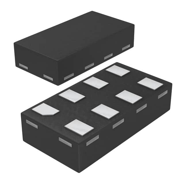
The 74LVC1G99GF,115 is available in a small form factor SOT753 package. It is typically sold in reels or tubes containing a quantity of 3000 units.
Specifications
- Supply Voltage Range: 1.65V to 5.5V
- Input Voltage Range: 0V to VCC
- Output Voltage Range: 0V to VCC
- Operating Temperature Range: -40°C to +125°C
- Propagation Delay: 3.8ns (typical)
- Maximum Quiescent Current: 10μA
Pin Configuration
The 74LVC1G99GF,115 features a total of six pins arranged as follows:
____
   A1 |    | VCC
   B1 |    | Y1
   GND |____| A2
        B2
        Y2
Functional Features
The primary function of the 74LVC1G99GF,115 is to perform logical AND/OR operations on two input signals (A and B) and provide the output (Y) based on the selected mode. It supports both positive and negative logic levels.
Advantages and Disadvantages
Advantages
- Low power consumption
- High-speed operation
- Wide operating voltage range
- Compact package size
Disadvantages
- Limited number of inputs and outputs
- Not suitable for complex logic operations
Working Principles
The 74LVC1G99GF,115 utilizes CMOS technology to achieve low power consumption and high-speed operation. It consists of transistors that act as switches, allowing or blocking the flow of current based on the input signals. The logical AND/OR operations are performed by combining these transistor switches.
Application Field Plans
The 74LVC1G99GF,115 finds applications in various fields, including: 1. Consumer electronics 2. Automotive systems 3. Industrial automation 4. Communication devices 5. Medical equipment
Alternative Models
Several alternative models with similar functionality are available in the market. Some notable alternatives to the 74LVC1G99GF,115 include: - SN74LVC1G99DBVR - MC74VHC1G99DTT1G - TC7SZU04FU
These alternatives can be considered based on specific requirements and availability.
In conclusion, the 74LVC1G99GF,115 is a versatile logic gate IC that offers high-speed operation, low power consumption, and wide voltage range. Its compact package makes it suitable for various applications in different industries.
तकनीकी समाधानों में 74LVC1G99GF,115 के अनुप्रयोग से संबंधित 10 सामान्य प्रश्नों और उत्तरों की सूची बनाएं
Sure! Here are 10 common questions and answers related to the application of 74LVC1G99GF,115 in technical solutions:
Q1: What is the function of the 74LVC1G99GF,115? A1: The 74LVC1G99GF,115 is a single 8-input multiplexer/demultiplexer with three-state outputs. It can be used to select one of eight input signals and route it to the output.
Q2: What is the operating voltage range for the 74LVC1G99GF,115? A2: The operating voltage range for the 74LVC1G99GF,115 is from 1.65V to 5.5V.
Q3: How many inputs does the 74LVC1G99GF,115 have? A3: The 74LVC1G99GF,115 has 8 inputs.
Q4: Can the 74LVC1G99GF,115 be used as a demultiplexer? A4: Yes, the 74LVC1G99GF,115 can be used as both a multiplexer and a demultiplexer.
Q5: What is the maximum output current of the 74LVC1G99GF,115? A5: The maximum output current of the 74LVC1G99GF,115 is 32mA.
Q6: Does the 74LVC1G99GF,115 have three-state outputs? A6: Yes, the 74LVC1G99GF,115 has three-state outputs, which means that the outputs can be disabled or put into a high-impedance state.
Q7: Can the 74LVC1G99GF,115 be cascaded to increase the number of inputs? A7: Yes, multiple 74LVC1G99GF,115 can be cascaded together to increase the number of inputs.
Q8: What is the propagation delay of the 74LVC1G99GF,115? A8: The propagation delay of the 74LVC1G99GF,115 is typically around 3.5ns.
Q9: Is the 74LVC1G99GF,115 compatible with other logic families? A9: Yes, the 74LVC1G99GF,115 is compatible with both CMOS and TTL logic families.
Q10: Can the 74LVC1G99GF,115 be used in battery-powered applications? A10: Yes, the 74LVC1G99GF,115 can be used in battery-powered applications as it operates at low voltage and has low power consumption.
Please note that these answers are general and may vary depending on specific application requirements.