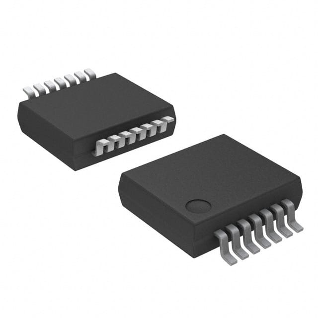
74HC58DB,118
Basic Information Overview
- Category: Integrated Circuit (IC)
- Use: Digital Logic IC
- Characteristics: High-speed operation, low power consumption, compatibility with TTL levels, wide operating voltage range
- Package: SOIC (Small Outline Integrated Circuit)
- Essence: 8-bit multiplexer/demultiplexer
- Packaging/Quantity: Tape and Reel, 2500 units per reel
Specifications
- Supply Voltage Range: 2V to 6V
- Input Voltage Range: 0V to VCC
- Output Voltage Range: 0V to VCC
- Operating Temperature Range: -40°C to +125°C
- Propagation Delay Time: 15 ns (typical)
- Input Capacitance: 3.5 pF (typical)
- Output Current: ±25 mA
Detailed Pin Configuration
- A0 - Address Input 0
- A1 - Address Input 1
- A2 - Address Input 2
- E - Enable Input
- Y0 - Multiplexer Output 0
- Y1 - Multiplexer Output 1
- Y2 - Multiplexer Output 2
- GND - Ground
- Y3 - Multiplexer Output 3
- Y4 - Multiplexer Output 4
- Y5 - Multiplexer Output 5
- Y6 - Multiplexer Output 6
- Y7 - Multiplexer Output 7
- VCC - Supply Voltage
Functional Features
- 8-bit multiplexer/demultiplexer with three address inputs (A0, A1, A2) for selecting one of the eight data inputs (Y0-Y7) to be routed to the output.
- Enable input (E) controls the operation of the device. When E is high, the outputs are in a high-impedance state.
- Compatible with TTL levels, allowing easy integration with existing digital logic circuits.
- High-speed operation and low power consumption make it suitable for various applications.
Advantages
- Wide operating voltage range allows flexibility in different power supply configurations.
- High-speed operation enables efficient data processing in time-critical applications.
- Low power consumption helps in reducing overall system energy requirements.
- Compatibility with TTL levels simplifies integration with existing digital systems.
Disadvantages
- Limited number of address inputs restricts the number of selectable data inputs.
- Propagation delay time may affect real-time applications requiring immediate response.
Working Principles
The 74HC58DB,118 is an 8-bit multiplexer/demultiplexer IC that operates based on the address inputs (A0-A2) and the enable input (E). The three address inputs determine which of the eight data inputs (Y0-Y7) will be routed to the output. When the enable input is high, the outputs are in a high-impedance state, allowing other devices to control the bus.
Detailed Application Field Plans
The 74HC58DB,118 can be used in various applications, including: 1. Data routing and selection in microcontrollers and digital processors. 2. Address decoding in memory systems. 3. Signal multiplexing in communication systems. 4. Input/output expansion in embedded systems. 5. Control signal routing in industrial automation.
Detailed and Complete Alternative Models
Some alternative models that offer similar functionality to the 74HC58DB,118 include: - CD4051B: 8-channel analog multiplexer/demultiplexer IC - SN74LS151: 8-input multiplexer IC - MC14051B: 8-channel analog multiplexer/demultiplexer IC
(Note: The above list is not exhaustive and there are other alternative models available in the market.)
In conclusion, the 74HC58DB,118 is a versatile 8-bit multiplexer/demultiplexer IC with high-speed operation, low power consumption, and compatibility with TTL levels. Its wide operating voltage range and compact SOIC package make it suitable for various digital logic applications. However, its limited address inputs and propagation delay time should be considered when designing real-time systems.
तकनीकी समाधानों में 74HC58DB,118 के अनुप्रयोग से संबंधित 10 सामान्य प्रश्नों और उत्तरों की सूची बनाएं
Sure! Here are 10 common questions and answers related to the application of 74HC58DB,118 in technical solutions:
Q: What is the 74HC58DB,118? A: The 74HC58DB,118 is a high-speed CMOS 8-bit addressable latch with three-state outputs.
Q: What are the typical applications of the 74HC58DB,118? A: It is commonly used in applications such as address decoding, data storage, and bus interfacing.
Q: What is the maximum operating voltage for the 74HC58DB,118? A: The maximum operating voltage is 6 volts.
Q: How many addressable latches are there in the 74HC58DB,118? A: The 74HC58DB,118 has 8 addressable latches.
Q: What is the output type of the 74HC58DB,118? A: The outputs of the 74HC58DB,118 are three-state outputs.
Q: What is the maximum clock frequency supported by the 74HC58DB,118? A: The maximum clock frequency is typically around 25 MHz.
Q: Can the 74HC58DB,118 be cascaded to increase the number of addressable latches? A: Yes, multiple 74HC58DB,118 chips can be cascaded together to increase the number of addressable latches.
Q: What is the power supply range for the 74HC58DB,118? A: The power supply range is typically between 2 volts and 6 volts.
Q: Does the 74HC58DB,118 have any built-in protection features? A: Yes, it has built-in protection against electrostatic discharge (ESD) and excessive power dissipation.
Q: What is the package type of the 74HC58DB,118? A: The 74HC58DB,118 is available in various package types, such as SOIC, TSSOP, and SSOP.
Please note that these answers are general and may vary depending on the specific datasheet and manufacturer's specifications for the 74HC58DB,118.


