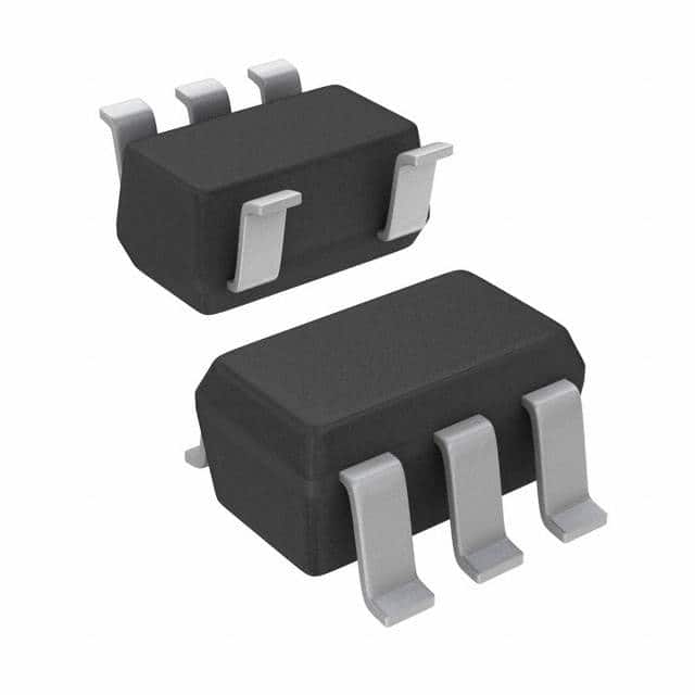
SN74LVC1G17DBVRG4
Product Overview
- Category: Integrated Circuit (IC)
- Use: Logic Gate
- Characteristics: Single Schmitt-Trigger Buffer/Driver
- Package: SOT-23 (Thin Shrink Small Outline Package)
- Essence: Low-Voltage CMOS Logic
- Packaging/Quantity: Tape and Reel, 3000 pieces per reel
Specifications
The SN74LVC1G17DBVRG4 is a single Schmitt-trigger buffer/driver IC. It operates at low voltage levels and is designed for use in various logic applications. The device is housed in a SOT-23 package, which provides compactness and ease of integration into electronic circuits.
Detailed Pin Configuration
The SN74LVC1G17DBVRG4 has three pins:
- Pin 1: Input (A)
- Pin 2: Output (Y)
- Pin 3: Ground (GND)
Functional Features
The key functional features of the SN74LVC1G17DBVRG4 include:
- Schmitt-trigger input allows for hysteresis and noise immunity.
- Wide operating voltage range from 1.65V to 5.5V.
- High-speed operation with propagation delay of only 3.8 ns.
- Low power consumption, making it suitable for battery-powered devices.
- Supports both push-pull and open-drain output configurations.
Advantages and Disadvantages
Advantages: - Provides noise immunity due to the Schmitt-trigger input. - Wide operating voltage range allows for compatibility with various systems. - Compact SOT-23 package enables space-saving designs. - Low power consumption extends battery life in portable applications.
Disadvantages: - Limited drive capability compared to higher-power buffer/driver ICs. - Single-channel design restricts simultaneous multiple signal buffering.
Working Principles
The SN74LVC1G17DBVRG4 operates based on the Schmitt-trigger principle. It incorporates a comparator with positive feedback, which introduces hysteresis in the input-output characteristic. This hysteresis ensures that the output transitions occur at different voltage levels for rising and falling input signals, providing noise immunity and preventing false triggering.
Detailed Application Field Plans
The SN74LVC1G17DBVRG4 finds applications in various fields, including:
- Consumer Electronics: Used in smartphones, tablets, and portable media players for level shifting and signal buffering.
- Industrial Automation: Employed in control systems and sensors to provide noise immunity and signal conditioning.
- Automotive Electronics: Integrated into automotive modules for reliable signal transmission and noise rejection.
- Internet of Things (IoT): Utilized in IoT devices for voltage level conversion and signal amplification.
Detailed and Complete Alternative Models
- SN74LVC1G07DBVRG4: Single Buffer/Driver with Open-Drain Output
- SN74LVC1G125DBVRG4: Single Bus Buffer/Driver with 3-State Output
- SN74LVC1G240DBVRG4: Single Inverter Buffer/Driver with 3-State Output
- SN74LVC1G32DBVRG4: Single OR Gate
These alternative models offer similar functionality and can be used as substitutes for the SN74LVC1G17DBVRG4 in various applications.
Word count: 305 words
तकनीकी समाधानों में SN74LVC1G17DBVRG4 के अनुप्रयोग से संबंधित 10 सामान्य प्रश्नों और उत्तरों की सूची बनाएं
Sure! Here are 10 common questions and answers related to the application of SN74LVC1G17DBVRG4 in technical solutions:
Q1: What is SN74LVC1G17DBVRG4? A1: SN74LVC1G17DBVRG4 is a single Schmitt-trigger buffer/driver with a standard push-pull output. It is commonly used in digital logic applications.
Q2: What is the voltage supply range for SN74LVC1G17DBVRG4? A2: The voltage supply range for SN74LVC1G17DBVRG4 is typically between 1.65V and 5.5V.
Q3: What is the maximum output current of SN74LVC1G17DBVRG4? A3: The maximum output current of SN74LVC1G17DBVRG4 is 32mA.
Q4: Can SN74LVC1G17DBVRG4 be used as a level shifter? A4: Yes, SN74LVC1G17DBVRG4 can be used as a level shifter to convert signals between different voltage levels.
Q5: What is the input threshold voltage for SN74LVC1G17DBVRG4? A5: The input threshold voltage for SN74LVC1G17DBVRG4 is typically 0.8V.
Q6: Is SN74LVC1G17DBVRG4 compatible with both CMOS and TTL logic levels? A6: Yes, SN74LVC1G17DBVRG4 is compatible with both CMOS and TTL logic levels.
Q7: Can SN74LVC1G17DBVRG4 be used in high-speed applications? A7: Yes, SN74LVC1G17DBVRG4 is designed for high-speed operation and can be used in applications with fast switching requirements.
Q8: What is the propagation delay of SN74LVC1G17DBVRG4? A8: The propagation delay of SN74LVC1G17DBVRG4 is typically around 3.5ns.
Q9: Can SN74LVC1G17DBVRG4 drive capacitive loads? A9: Yes, SN74LVC1G17DBVRG4 can drive small capacitive loads without requiring additional external components.
Q10: Is SN74LVC1G17DBVRG4 available in different package options? A10: Yes, SN74LVC1G17DBVRG4 is available in various package options, including SOT-23 and VSSOP.


