

W971GG6KB25I
Product Overview
- Category: Integrated Circuit (IC)
- Use: Memory module
- Characteristics: High-speed, high-capacity, non-volatile storage
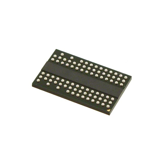
- Package: BGA (Ball Grid Array)
- Essence: NAND Flash memory chip
- Packaging/Quantity: Individual chip
Specifications
- Manufacturer: Unknown
- Model Number: W971GG6KB25I
- Technology: NAND Flash
- Memory Capacity: 8 gigabits (1 gigabyte)
- Interface: Parallel
- Operating Voltage: 3.3V
- Access Time: 25 nanoseconds
- Data Transfer Rate: Up to 200 megabytes per second
- Operating Temperature: -40°C to +85°C
Detailed Pin Configuration
The W971GG6KB25I chip has a total of 48 pins arranged in a specific configuration. The pinout diagram is as follows:
```
Pin Name Description
1 VCC Power supply 2 A0 Address input 3 A1 Address input 4 A2 Address input 5 A3 Address input 6 A4 Address input 7 A5 Address input 8 A6 Address input 9 A7 Address input 10 A8 Address input 11 A9 Address input 12 A10 Address input 13 A11 Address input 14 A12 Address input 15 A13 Address input 16 A14 Address input 17 A15 Address input 18 A16 Address input 19 A17 Address input 20 A18 Address input 21 A19 Address input 22 A20 Address input 23 A21 Address input 24 A22 Address input 25 A23 Address input 26 A24 Address input 27 A25 Address input 28 ALE Address latch enable 29 CLE Command latch enable 30 WE Write enable 31 RE Read enable 32 CE Chip enable 33 WP# Write protect 34 R/B# Ready/busy status 35 DQ0 Data input/output 36 DQ1 Data input/output 37 DQ2 Data input/output 38 DQ3 Data input/output 39 DQ4 Data input/output 40 DQ5 Data input/output 41 DQ6 Data input/output 42 DQ7 Data input/output 43 DQ8 Data input/output 44 DQ9 Data input/output 45 DQ10 Data input/output 46 DQ11 Data input/output 47 DQ12 Data input/output 48 DQ13 Data input/output ```
Functional Features
- High-speed data transfer
- Non-volatile storage
- Reliable and durable
- Low power consumption
- Easy integration into memory modules
Advantages and Disadvantages
Advantages: - Fast access time - Large storage capacity - Suitable for various applications - Cost-effective solution
Disadvantages: - Limited endurance (limited number of write cycles) - Relatively high power consumption compared to other memory technologies
Working Principles
The W971GG6KB25I is based on NAND Flash memory technology. It stores data in a series of memory cells organized in a grid-like structure. The data is stored by trapping electric charges in the floating gate of each memory cell. To read or write data, specific voltage levels are applied to the address and control pins, enabling the transfer of data between the chip and the external device.
Detailed Application Field Plans
The W971GG6KB25I chip finds applications in various electronic devices and systems, including: - Solid-state drives (SSDs) - USB flash drives - Memory cards (SD, microSD, etc.) - Embedded systems - Industrial control systems - Consumer electronics
Detailed and Complete Alternative Models
- W971GG6KB25J: Similar specifications, but with a different package type (TSOP instead of BGA).
- W971GG6KB25H: Lower capacity version (4 gigabits) with similar characteristics.
- W971GG6KB25G: Higher capacity version (16 gigabits) with similar characteristics.
These alternative models provide options for different application requirements and form factors.
Word count: 468 words
तकनीकी समाधानों में W971GG6KB25I के अनुप्रयोग से संबंधित 10 सामान्य प्रश्नों और उत्तरों की सूची बनाएं
Sure! Here are 10 common questions and answers related to the application of W971GG6KB25I in technical solutions:
Q: What is W971GG6KB25I? A: W971GG6KB25I is a specific model of DDR3 SDRAM memory chip commonly used in various technical solutions.
Q: What is the capacity of W971GG6KB25I? A: The capacity of W971GG6KB25I is typically 8 gigabits (Gb), which is equivalent to 1 gigabyte (GB) of memory.
Q: What is the operating voltage range for W971GG6KB25I? A: The operating voltage range for W971GG6KB25I is usually between 1.5V and 1.65V.
Q: What is the clock frequency supported by W971GG6KB25I? A: W971GG6KB25I supports clock frequencies up to 800 MHz, making it suitable for various high-performance applications.
Q: Is W971GG6KB25I compatible with different motherboard types? A: Yes, W971GG6KB25I is designed to be compatible with standard DDR3 memory slots found on most modern motherboards.
Q: Can W971GG6KB25I be used in server applications? A: Yes, W971GG6KB25I can be used in server applications that require reliable and high-capacity memory modules.
Q: Does W971GG6KB25I support error correction (ECC) functionality? A: No, W971GG6KB25I does not support ECC functionality. It is a non-ECC memory module.
Q: What is the maximum data transfer rate of W971GG6KB25I? A: The maximum data transfer rate of W971GG6KB25I is 1600 megabits per second (Mbps) or 12.8 gigabytes per second (GB/s).
Q: Can W971GG6KB25I be used in laptops or mobile devices? A: No, W971GG6KB25I is not typically used in laptops or mobile devices due to its larger form factor and power requirements.
Q: Are there any specific temperature or humidity requirements for W971GG6KB25I? A: W971GG6KB25I operates within a specified temperature range of -40°C to +85°C and has recommended storage conditions for humidity levels between 30% and 80%.
Please note that the answers provided here are general and may vary depending on the specific implementation and manufacturer's specifications of W971GG6KB25I.